Recreating a very capable but mostly forgotten single board computer for industrial control applications | Last updated Mar 27 2025
Disclaimer: I have not worked for Control Universal at any point in my history and do not have any original CU boards. All of the information here is therefore pieced-together from online research, conversations and reverse-engineering. If anything here is incorrect please let me know and I will endeavour to correct. Additionally, while preliminary tests of this board seem to indicate all is working with the design, further testing will confirm long term stability and comprehensive functionality.
Background & A Brief History of Control Universal
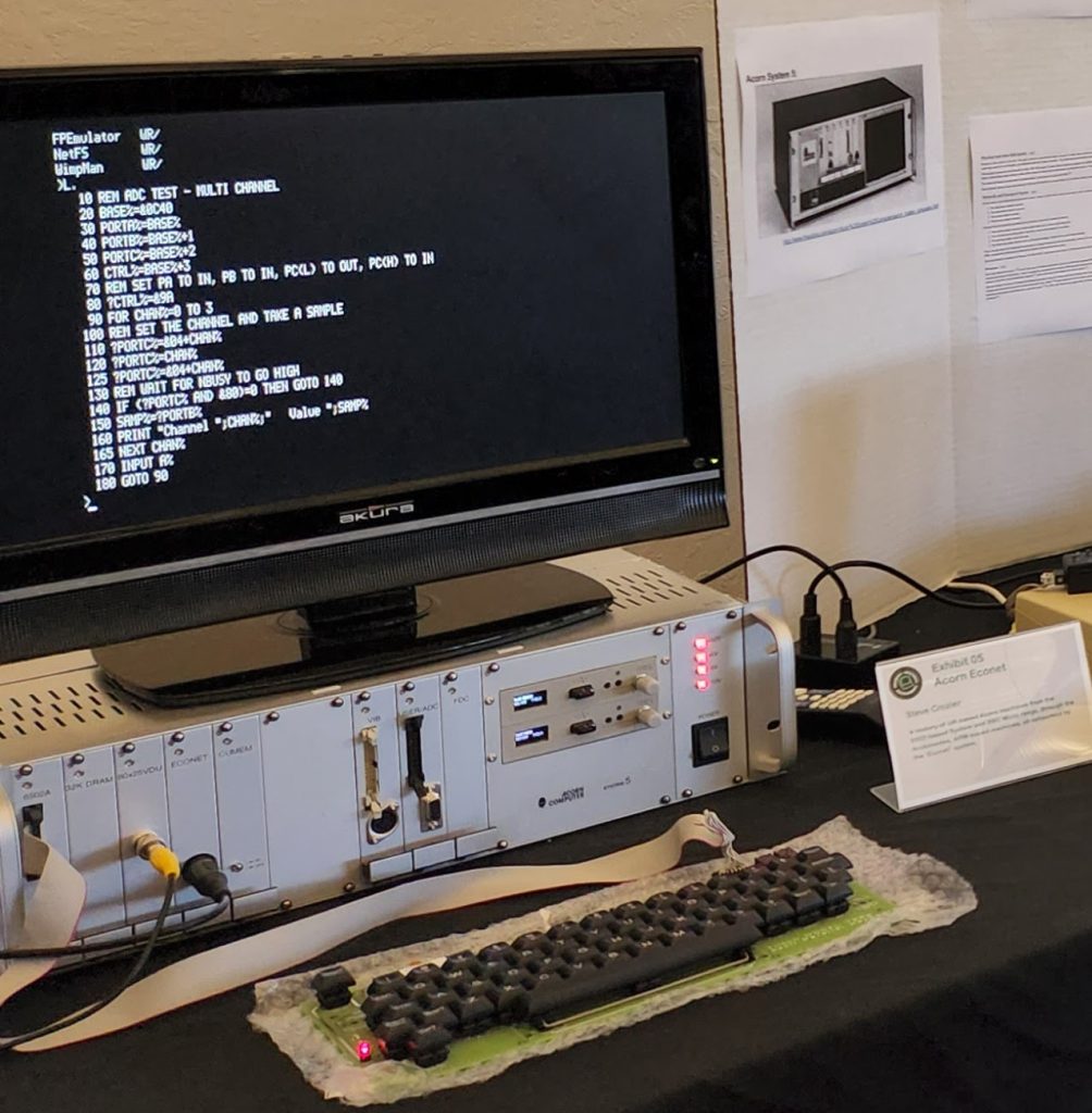
A while ago I put together a clone of an Acorn System 5. This is a EuroCard format / rack-mount system from Acorn, which pre-dates their hugely successful BBC Micro range of computers. Most of the replica PCBs were sourced from Chris Oddy (much credit for his excellent work).
One of the cards in my System 5 is the CUMEM board, which was developed by a third-party company, Control Universal. This then whet my appetite to learn more about this company.
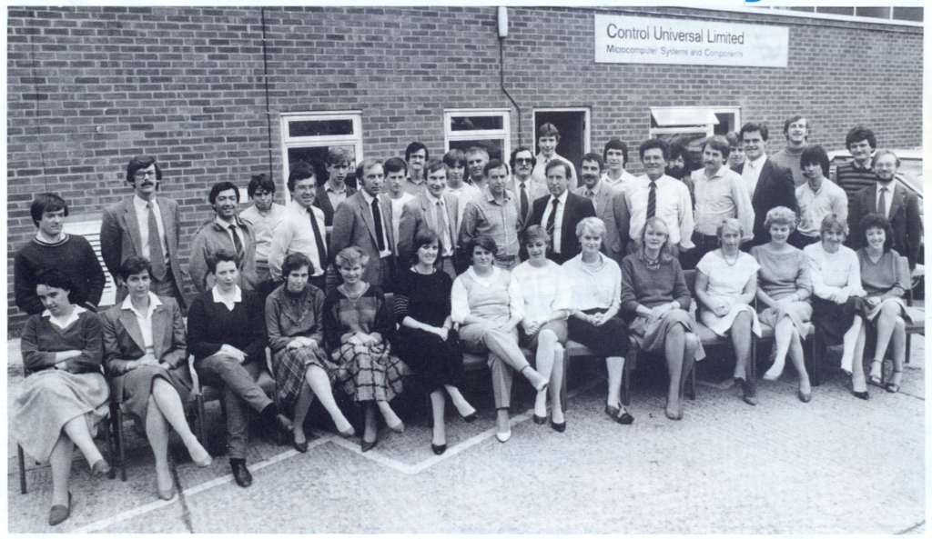
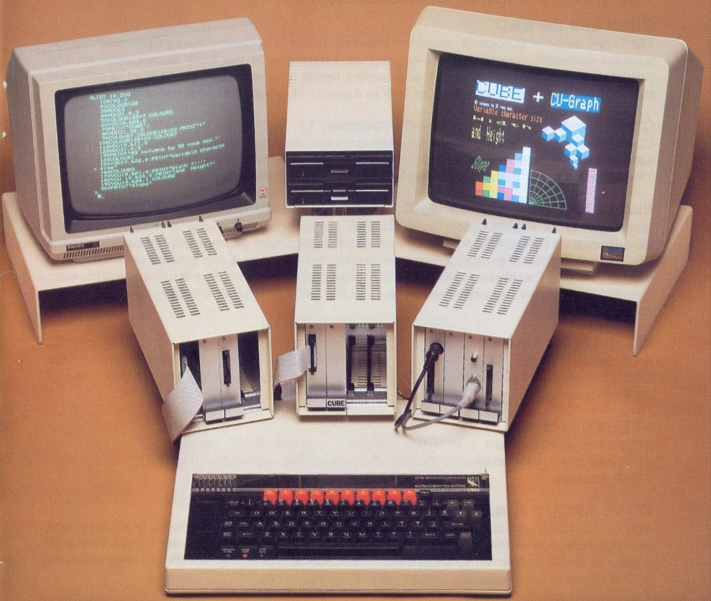
With some information from Chris’ site and also various searches I learned that Control Universal (CU) was a small company. Much like Acorn, CU was based in Cambridge, UK, remaining squarely focussed on computers for industrial control applications (remembering this all pre-dated low-cost and reliable PLCs). The company was formed in the late 1970s, initially selling Rockwell AIM-65 systems, and later on being a reseller for the Acorn System range of industrial computers, as Acorn shifted focus to the hugely successful educational and home computer segment. At the same time, CU started developing their own range of interface, memory and other boards which were compatible with the Acorn System bus.
After a while CU developed their own processor cards for industrial control applications. These remained in the EuroCard form factor and were known as EuroCUBE-65 and EuroCUBE-09, being based on the 6502 and 6809 processors respectively and having ROM, RAM and some I/O onboard. At this point CU had a wide range of peripheral cards from hi-res graphics to disk interface, memory, servo, analog and digital IO cards.
EuroCUBE and the EuroBEEB
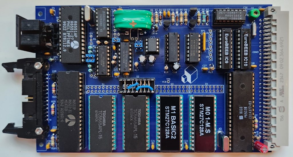
What particularly sparked my interest here was a variant of the EuroCUBE-65 known as the EuroBEEB. Using the 6502 hardware the card was configured with a custom Machine Operating System (MOS), a genuine Acorn BASIC 2 ROM and 16KB CMOS static RAM. Effectively this would look like a very cut-down BBC Micro which was accessed over a serial interface. Much of the memory map, interfaces and language were compatible, except it was missing onboard graphics. However, with a very clever terminal software running on the BBC Micro *EURO graphics could be routed back to the BBC for display there.
The EuroBEEB could therefore be considered as a next-generation System machine, taking some of the best parts of the BBC Micro and adding them to an embedded machine. It didn’t stop there though… the MOS ROM could be generated to contain different options (local keyboard support, Teletext or HiRes graphics card support, or Control BASIC extensions allowing convenient access to ADCs, IO etc from within BASIC 2).
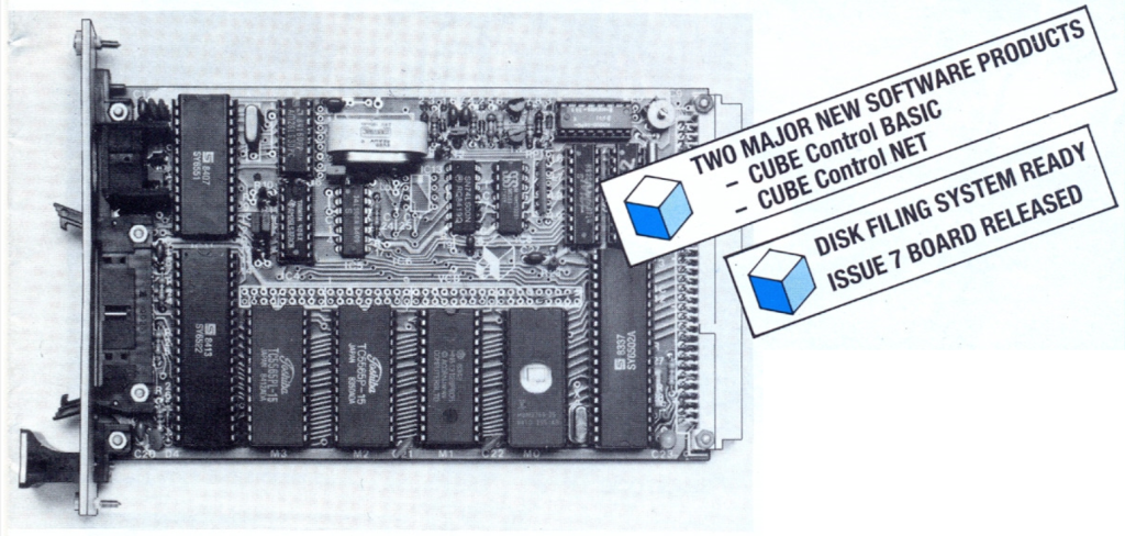
The EuroBEEB Architecture
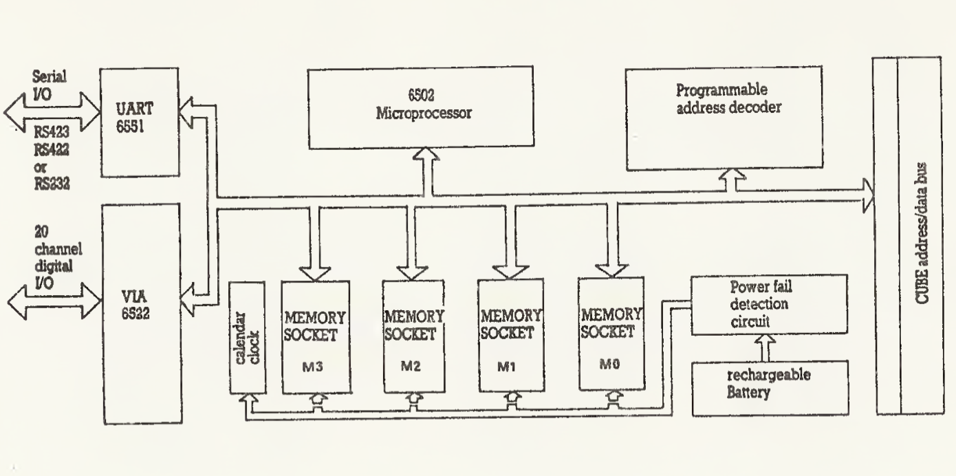
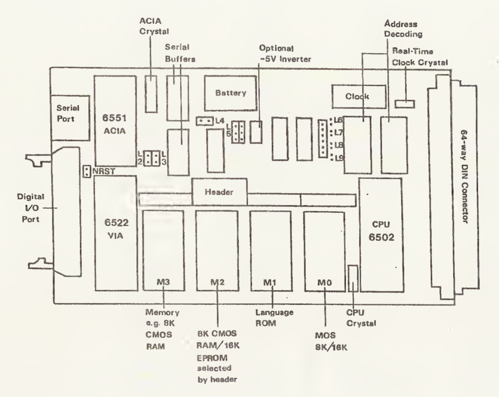
The architecture is actually a pretty simple/straightforward 6502 system. At the low end of the memory map is an 8K RAM (M3: needed for zero page and stack). Then another 8K RAM (M2: which can be replaced with an EEPROM if different S2 configuration jumper/link set is used). Then we have a gap for expansion card I/O, a 16K BASIC 2 ROM from the BBC Micro (M1) and a 16K MOS ROM containing operating system, utilities (configurable on generation) at the top end of the memory map (M0). More on the memory map later, when we get onto memory decoding.
In terms of peripherals there is a 6551 ACIA (UART) for communication with the terminal interface (can be a BBC Micro or regular ASCII terminal), a 6522 VIA for digital I/O (one line is reserved, everything else is available) and a M3002 real time clock/calendar IC. The RTC and RAM are low-power CMOS devices, and the board contains a battery back up for these, meaning that programs can be retained through a power cycle. Some power fail detection circuitry ensures devices are disabled as the supply drops / before bad writes and corruption occurs.
All of this is packaged into a very compact 160x100mm EuroCard layout (hence the Euro… name). Condensing into this form factor was quite a feat for early 1980’s technology, so hats-off to whoever did the original board layout. This wouldn’t have been possible using discrete logic for the address decoding, and two PROMs are used (IC9,10) which I’ll talk more about later.
Recreating the EuroBEEB
At this point I had decided that I needed a EuroBEEB to add to my collection of all computers Acorn-related. However sourcing such a rare machine would be difficult. Since these were not home, education or games machines, and used for industrial control applications, many will have been upgraded to PLCs and simply scrapped back in the mid-late 1990’s. You may have noted the NiCd battery (top, centre) on the image above. I previously mentioned, these boards have battery backup for the real-time clock/calendar and 16K CMOS RAM retention. As you might imagine, 40 year-old NiCd batteries tend to “do their thing”, leaking electrolytes and corroding PCB traces. As a result, even the ones that do exist are often in a rather bad shape and often not functional.
Fortunately there are a few sources of information on these machines including Cris Oddy’s site, Jonathan Harston’s MDFS.NET and of course the stardot forums. From piecing the available information together (including rather great documentation in the original EuroBEEB Manual, I decided to embark upon re-creating the EuroBEEB.
Now, before going any further I want to point out that this is not a trace-for-trace replica board. Since I don’t have an original issue 7 board to de-populate it’s not been possible to make this super-accurate to the original. Furthermore, the address decoding on the original board was done by two 82LS147 PROMs (IC9, 10). Since these are pretty much unobtanium to source, and programming them is another significant challenge, I decided to replace them with 16V8D GALs. This means that the board is not a direct replica and parts should not be simply transferred from a corroded existing PCB to the new one (you have all been warned!). That said, the board is address, software and functionally-compatible with the originals and I have kept the component locations approximately the same. I have made a few improvements (see later), so I’m calling this an ISSUE 8 evolution or re-creation but not a clone or replica.
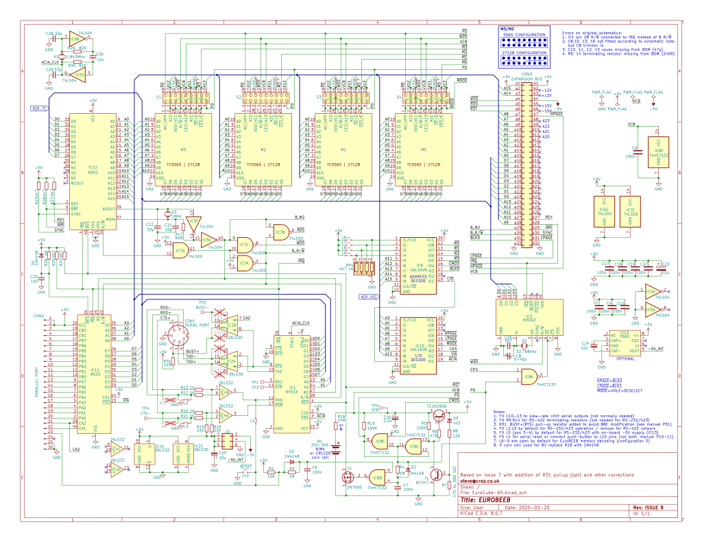
Redrawing the Schematic
The first step was to redraw the schematic. This was basically reconstructed from three sources:
- The EuroBEEB manual last page (arguably the most accurate – ISSUE 7 board, but a pretty poor scan with some illegible lines)
- The EuroCUBE-65 user manual (better scan but not latest issue – can’t quite recall where I sourced this from)
- Lee Davidson’s redrawn schematic (better quality but the drawing is marked as ‘not complete’, also unknown pedigree since it has the ACIA clock from the ISSUE 7 board but has a divided 4MHz clock for the 6502, presumably 2MHz can be selected by L11, if using a 6502A or B)
The configuration I chose to draw up was based on the ISSUE 7 schematic (fixed 1MHz clock), but with some errors corrected and some additions made. Note that to be consistent with the ISSUE 7 PCB, S2 is fitted as a 18-pin DIL header, so that a configuration jumper block can be fitted to select M2 as either a 8K RAM (TC5565) or 8K EPROM (27128); the idea here being that once your application is developed, it can be transferred to an EPROM and auto-loaded at boot (covered in the manual). This can then alleviate the need for the battery backup (of course, losing the RTC battery backup as a consequence). I won’t go into the detail of the additions right now – these are covered on the schematic and I’ll explain more during the breadboard prototype testing (see below). I should mention that T1..T3 have been replaced with more commonplace alternatives that are easier to source. I should also mention (in case I don’t do so later) that the 6502 should NOT be replaced with the (still in manufacture by WDC) CMOS 65C02. The clock configuration is different and it won’t work in this application.
Above you can see an export of the schematic (click to zoom). For a better quality PDF and the source files in GitHub along with PDF data sheets for all of the key parts, refer to my GitHub repo.
Address Decoding GALs
The greatest challenge was to replace the two address decoding PROMS (IC9, 10) with GALs. This involved figuring out the original memory decoding logic, building that into PLD logic description files, for compilation into JED files using WinCUPL. Given my skills with hardware description language are fairly sketchy, and confidence was low, I decided to build a device from an Arduino Mega to test the programmed devices (think of it as unit testing hardware). Fortunately there is rich source of information on how the address decoding works, between the files on mdfs.net and the information in the EuroBEEB manual. IC9 decoded the top 5 bits of memory and can be configured for up to 16 different memory maps using L6 through L9.
Update: There are now two versions of the IC9 PLD and JED files (version 6). There aren’t enough gates to decode all maps in one device, so there are now two programming options. IC9a is the file you want for a default EuroBEEB build, which decodes maps 0x0 through 0x9 (0 being the standard/default). IC9b is an alternative GAL programming that decodes maps 0xA through 0xE for alternative configurations (note this will not work in a standard EuroBEEB). I have tested and can confirm the default EuroBEEB memory map is working and all other maps match the descriptions in the file comments. Note the maps marked ‘reserved’ in the manual are unknown and simply not decoded.
Outputs of the IC9 GAL are generally a bunch of active-low memory select lines and an I/O select line which then heads off to IC10 for further decoding.
IC10 then takes the I/O select line and the next-lower 8 address lines to decode specific I/O addresses for peripherals such as the ACIA, VIA, RTC and some lines which are published on the expansion connector (presumably to make address decoding on external peripherals easier). Note the active low M0OE (memory zero output enable) line. ~M0 (connected to chip enable at the ROM) enables the MOS ROM from 0xC000 to 0xCFFF and then again from 0xE000 to 0xFFFF (block D being reserved for external peripherals). However ~M0OE is used to further disable the ROM (connected to the ROM’s output enable line) from 0xFE00 through 0xFEFF to avoid conflicts with onboard peripherals. The M0 ROM is re-enabled 0xFF00 through 0XFFFF to allow the reset, IRQ, NMI vectors and so on to be read. This might sound complicated, but all of this should be pretty well documented with comments in the PLD files.
The GitHub repository contains both the PAL (source) and compiled (JED) files, since finding/configuring and using the right version of WinCUPL can be a PITA. The JED files can be programmed to 16V8Ds directly using a TL866 or other programmer of choice.
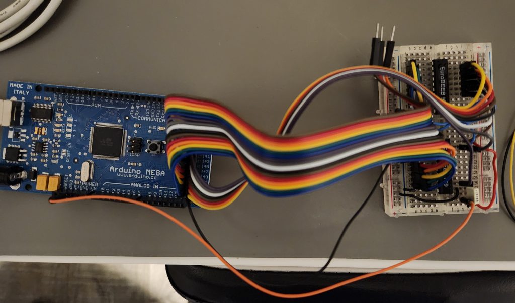
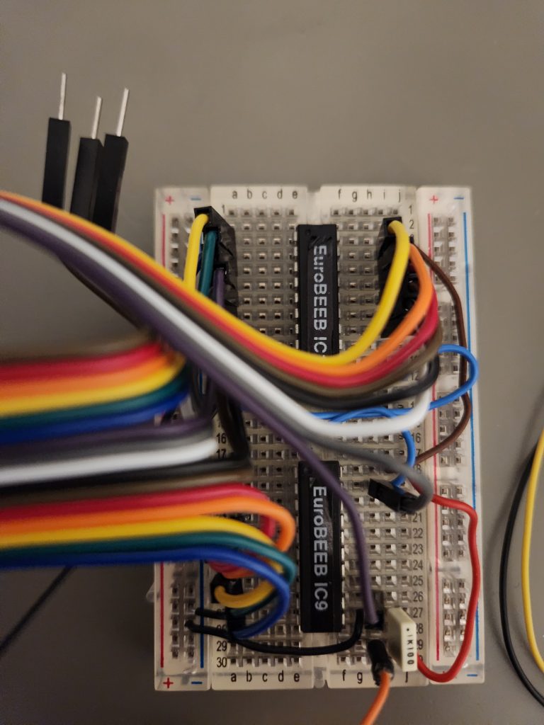
With GALs programmed the next stage was to test these in isolation. I decided to do this using an Arduino Mega to cycle through the entire address space and build out a text-based memory map whenever one of the output lines changes state (see the .INO file in the /AddressDecoderTester folder of the repo). Disclaimer: this is far from the most efficient code, but allowed me to use a choice of I/O lines for convenient wiring (not all pins need to be on the same ports). However exercising the full 64K address space takes only a few seconds, so I didn’t get hung up on optimisation. Here’s what the whole thing looks like hooked up on a small breadboard (click the images to see zoomed/full):
Decoded output when testing IC9:
Address decoding / memory mapper - Steve C - Dec 2024

CMOS RAM ----------------|
CMOS RAM ------------|
BASIC ROM -----|
MOS ROM --|
         ~M0  ~M1  ~M2  ~M3 ~CMOS ~BLK0 N/C ~IO
Address | E0 | E1 | E2 | E3 | E4 | E5 | E6 | E7
------------------------------------------------
0x0000 |  1 |  1 |  1 |  0 |  1 |  1 |  1 |  1
0x2000 |  1 |  1 |  0 |  1 |  1 |  1 |  1 |  1
0x4000 |  1 |  1 |  1 |  1 |  0 |  1 |  1 |  1
0x8000 |  1 |  0 |  1 |  1 |  0 |  1 |  1 |  1
0xC000 |  0 |  1 |  1 |  1 |  0 |  1 |  1 |  1
0xD000 |  1 |  1 |  1 |  1 |  0 |  0 |  1 |  1
0xE000 |  0 |  1 |  1 |  1 |  0 |  1 |  1 |  1
0xF800 |  0 |  1 |  1 |  1 |  0 |  1 |  1 |  0
0xFFFF |  0 |  1 |  1 |  1 |  0 |  1 |  1 |  0
------------------------------------------------
--Done---
and when testing IC10:
Address decoding / memory mapper - Steve C - Dec 2024


        ~M0  ~IO ~HPG ~LPG ~M0OE CKS ~VIA ~ACIA
Address| E0 | E1 | E2 | E3 | E4 | E5 | E6 | E7
------------------------------------------------
0x0000 |  1 |  1 |  1 |  1 |  0 |  0 |  1 |  1
0xC000 |  0 |  1 |  1 |  1 |  0 |  0 |  1 |  1
0xD000 |  1 |  1 |  1 |  1 |  0 |  0 |  1 |  1
0xE000 |  0 |  1 |  1 |  1 |  0 |  0 |  1 |  1
0xF800 |  0 |  0 |  1 |  1 |  0 |  0 |  1 |  1
0xFE00 |  0 |  0 |  1 |  0 |  1 |  0 |  0 |  1
0xFE10 |  0 |  0 |  1 |  0 |  1 |  0 |  1 |  0
0xFE18 |  0 |  0 |  1 |  0 |  1 |  1 |  1 |  1
0xFE20 |  0 |  0 |  1 |  0 |  1 |  0 |  1 |  1
0xFE80 |  0 |  0 |  0 |  1 |  1 |  0 |  1 |  1
0xFF00 |  0 |  0 |  1 |  1 |  0 |  0 |  1 |  1
0xFFFF |  0 |  0 |  1 |  1 |  0 |  0 |  1 |  1
------------------------------------------------
--Done---
Note that the tester code logs a line at 0x0000, whenever the outputs change state and at 0xFFFF. This means for example, that M3 is low from 0x0000 to 0x1FFF and transitions high from 0x2000 onwards.
With the memory decoding tested it’s time to start building the circuit up as a prototype on breadboards. I wouldn’t usually build up something so large on breadboards, but I wanted to be somewhat confident that this would work before investing so much time in laying out the PCB.
Breadboard Prototyping & Hardware Debugging
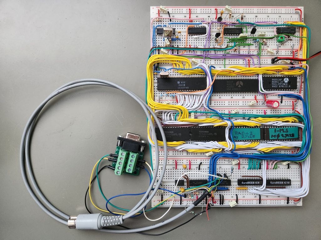
After many hours of inserting parts and cutting wires to length, this is what the prototype looks like:
The whole thing runs of a single +5V rail (bottom left is the 7660 which generates the -5V needed for RS232/423 serial comms). You can see that I’ve fitted both a DIN-5 plug and a DE9 so I could test with initially a PC terminal and then with a BBC Micro running the dedicated/special purpose *EURO terminal.
- Top-left/centre is the general purpose logic, reset and power supply monitor (there is space for the NiMh but not fitted here).
- Top-right is the M3002 RTC
- Centre-left is the 6502 CPU with VIA and ACIA
- Bottom-left/centre we have the serial interface
- Bottom-right are the two address decoding GALs from the previous step
I’d be lying if I were to say that getting this working was trivial. This is by far the largest thing I’ve prototyped on breadboard and I had to make extensive use of my DSLogic Pro32 logic analyser to resolve several issues:
- CKS connected to the wrong pin
- Bad 6502 (A7 line stuck)
- Bad M3002 (probably a fake part / all data lines stuck, causing a bus conflict, stuck IRQ and getting hot)
- Reversed data lines to the ACIA
- At least one address wire became dislodged (they’re very closely packed)
- RTS/CTS handshaking not working right on the serial link*
The bad 6502 and M3002 illustrate the challenges of sourcing out of production stock to build and maintain retro computers. Fortunately my 32 channel logic analyser has proven incredibly useful for debugging hardware of this nature. Blessed I could monitor all 16 address lines, all 8 data lines and have 8 free lines for clocks and control signals.
Debugging was also aided by writing some test code to exercise each peripheral in turn, reading a byte from the device into RAM (see the /HardwareDebug folder in the repo. The small compiled binary replaced the M0 MOS and was very handy in debugging. After several days of debugging I’m pleased to say it’s fully working (for reference the working board was pulling 320mA at 5.2V. Slightly higher than 5.0V was set to account for some small drops through wiring and the prototype breadboards).
Now seems to be a good time to mention some modifications/additions over the previous ISSUE 7 design. The first of these solves the handshaking issue above * and involves adding a 1K8 pull-up resistor (R31) from BUSY+ (RTS) to +5V. This is very briefly mentioned in the EuroBEEB manual (see page 51) as being needed at the BBC Micro end with this version of MOS. Rather than modifying all of my machines, it seems more appropriate to add at the EuroBEEB end. The second key modification is to replace the transistors with some compatible and more easily obtainable parts. Lastly I have added a second footprint to the PCB for a coin cell (CR1220) to be fitted instead of a NiMh battery. If a coin cell is used then R18 should be replaced with a 1N4148 or similar diode to prevent recharging (shown in the schematic and on the PCB silkscreen).
The only potentially troublesome issue that I’ve run into is with SAVEing and LOADing data using the BBC’s inbuilt disk drive (see this thread on StarDot). After a SAVE command is received, a binary-block transfer of memory occurs and the Beeb then deletes any existing file and writes to disk (vice-versa for LOAD). This works fine on my BBC Master 128 and Model B, but has been problematic on my B+ (currently being investigated).
PCB Layout
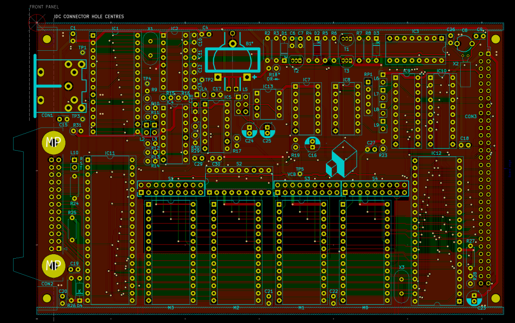
The PCB Layout was performed in KiCad 8 and all of the design files are included. I’ve reduced the track size from the original (to 0.2mm for most signals) to aid routing the vertical tracks, but kept the power lines nice and thick. It’s a 2-layer board with a flood-fill GND on top and bottom. The flood-fill doesn’t cover all of the memory IC pins, so that the S1-S4 grounded links don’t get filled (a slight hack). I tend to reduce the size of the thermal relief spokes to GND pads from the KiCad default to make soldering slightly easier. For anyone interested in peripheral cards, I also have a ‘template’ Eurocard project [to be added soon] with holes and DIN41612 connector accurately placed.
All of the non-polarized capacitors have a 2.54mm pad spacing on the footprint (I find these use the least real estate on the board), and the polarized capacitors use a 2mm (pretty standard for most electrolytics) pad spacing. While the original used tantalum caps (and these are still available if you want to be as authentic as possible) electrolytic caps should be fine, although C23 might benefit from being tantalum since there aren’t any close-by decoupling caps for IC12. All IC footprints are for sockets, and these are recommended (I tend to use dual-wipe sockets normally and turned pin for the memories, which tend to get more removal).
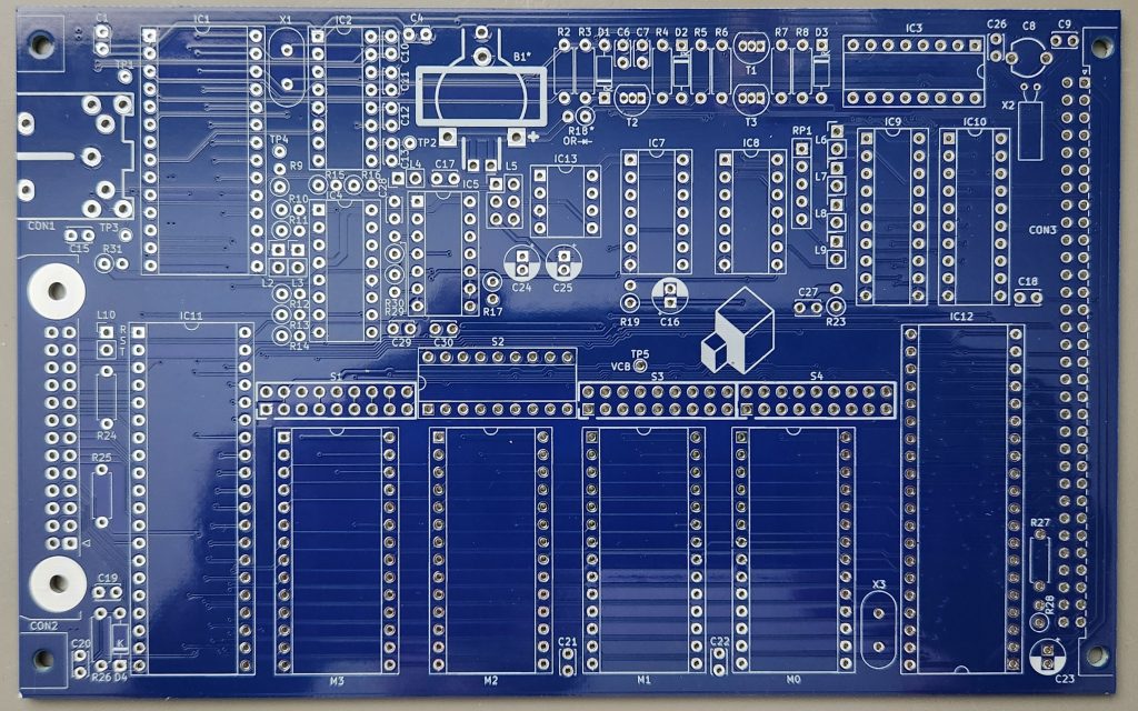
Design-wise the part layout is very similar to the original boards (noting IC12 remains upside-down compared to others). The part placement isn’t precise to the original (the keen-eye may notice that the gap between IC1 and IC2/4 is a little narrower than the original, to give more space around B1. B1 has pads for either the PCB mounted NiMh, or for a CR1220 3V coin cell in holder. R31 has been added between the left-side connectors. Where resistors were vertically mounted I’ve kept them that way for originality.
Manufacturing-wise I’ve gone with PCBway and the design files are available there for direct manufacture. I’ve chosen to have the boards manufactured with white silkscreen on blue soldermask. While today’s blue soldermask is a little glossier than the original I like the blue look of CU boards. On that note I read in one of the control universal newsletters that the 4MHz boards would be blue and the older 1MHz boards would remain in green soldermask. However I’ve seen examples of the original boards reversed from that norm so doubt CU ever actually adhered to that standard.
The repository includes all KiCad files along with a BOM (with suggested supplier links) and an interactive BOM to help with assembly. Note that the links to source parts are examples, and some such as the eBay links are likely to be stale when you come to source parts. The most difficult part to source is likely to be the M3002 real time clock, but there seem to be some sources in the UK, US and China. Note that the BOM doesn’t include IC sockets or go into detail about the link headers, which can be snapped to length from a single 40-pin long piece.
Assembly & Testing
Assembly can be in your preferred order. Use the interactive Bill of Materials (BOM) to identify the location/values of parts. To make ordering parts easier I’ve added some notes and potential sources to the CSV BOM. Both of these are in the \BOM folder of the repository. For me I like to start with the lowest profile parts and work up in height, for example:
- Diodes,
- Horizontally mounted resistors,
- IC sockets (noting that IC12 is upside-down compared to all other ICs),
- Ceramic capacitors and RTC crystal,
- Transistors (closely spaced pads, take care to avoid solder bridges) and resistor pack,
- Links and trimmer cap (noting that L6-9 can be left open/not fitted if using the default EuroBEEB memory map),
- Vertically mounted resistors, polarised capacitors, vertically mounted crystals,
- Connectors in order of height.
- Don’t forget to configure the S2 header as per the schematic (and the image below)
When you’re all done, it should look something like this (although I recommend preliminary testing with no battery fitted):
Here’s how it looks populated with either the NiMh or coin cell battery options. Alternatively a 3-cell NhMh could be mounted off-board on flying leads (to avoid the leakage risk if you really want the capacity of a rechargeable, since I expect the coin cell will deplete pretty quickly… TBC)
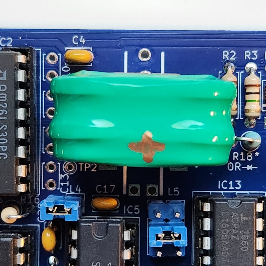
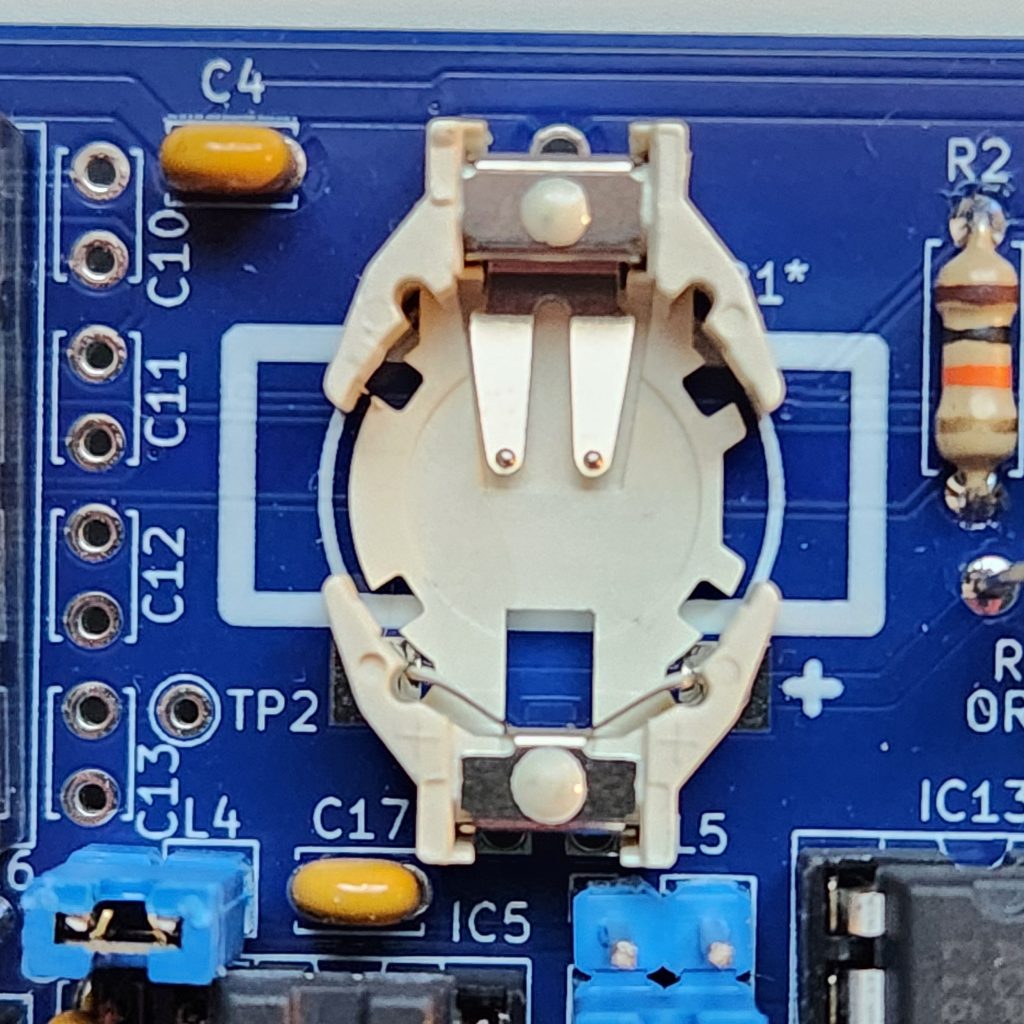
Testing should be pretty straightforward. First hook up external power to the +5V and GND connections current limited to 400mA. Powered on, the current draw should be around 350mA. If it’s significantly more that this, stop and investigate. You should have close to 5V on the VCB test point, -4 to -5V on the middle-right pin of L5. Clocks should be 1.84MHz measured on IC1 pin 3, 1MHz measured on IC5 pin 10 and approximately 32KHz measured on pins 2/3 of IC3 (although not particularly square). The RTC clock should be trimmed (C8 and optionally C26) for 256Hz at pin 15 of IC3, but this may not be possible until the clock is initialised (see code below).
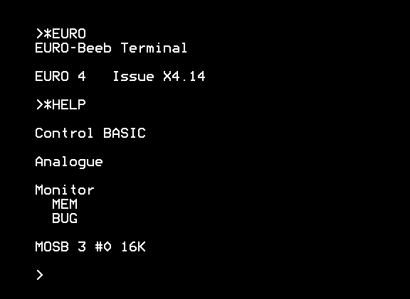
The next stage is to hook up a BBC Micro (running *EURO) or another terminal at 9600 baud, 8 data bits, no parity, 1 stop bit, RTS/CTS handshake to CON1. If all is good you should see something like this, with the *HELP command confirming that the utilities in the MOS ROM are available.
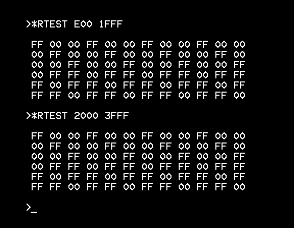
Next is to test the RAM. Fortunately inbuilt utilities can be used here *RTEST E00 1FFF will test the lower 8K (M2, omitting the area used by the MOS) and *RTEST 2000 3FFF will test the upper 8K (M3), and should show some results like this:
Next steps are to check the RTC and interrupt (internal timer) operation. This can be done with the following code. If all is well the clock should be counting up, and the timer counting up. This is set to just before midnight, so should roll over to 2nd Jan after a minute of operation.
10 REM Clock test code | S.C. | 2025
20 CLOCK$.="23:59:00"
30 DATE$.="01:01:84"
40 CLS
50 PRINT TAB(0,0);"TIME      DATE       TIMER"
60 PRINT TAB(0,1);CLOCK$,DATE$,TIME
70 GOTO 60With the clock working, the VIA ports A/B can be tested with either of these code blocks, the first progressively toggling all I/O and the second allowing pin by pin toggling. This is easily checked with a logic probe or scope on IC11 pins 2 through 17.
10 REM Port Test 1 | S.C. | 2025
20 OUTCH 0 TO 15
30 FOR I%=0 TO 15
40 FLIP I%
50 NEXT I%
60 GOTO 30
10 REM Port Test 2 | S.C. | 2025
20 OUTCH 0 TO 15
30 INPUT "CHANNEL ";I%
40 FLIP I%
50 GOTO 30With the basics working, you’re now free to go ahead creating automation applications in BBC Basic, using the manual as a reference. These three programs are on the Samples.SSD disk image (see repo).
Enclosure
Next steps are to figure out an enclosure. Verotec (US and UK) is the obvious point of contact for all hardware EuroCard related, but I feel I might have to do some hacking and/or 3d printing to get an enclosure as small as the originals. If anyone has ideas/designs then please let me know.
Known Issues
At this time the board has been tested and confirmed to be working on an Acorn BBC Micro Model B (issue 7) and a BBC Master (issue 2).
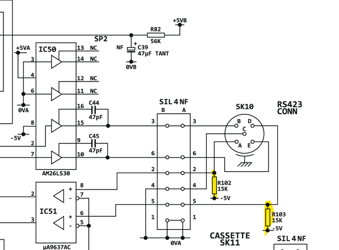
There is a known issue with the BBC Master (Issue 1) board, which was fixed on issue 2 (see stardot thread on the differences). If you encounter difficulties in communicating the board and have a BBC Master (issue 1 specifically) then 2x 15K resistors need to be fitted between the input signals and -5V. These are relatively easily attached to the pads of the SIL 4 NF block and a convenient -5V point.
Miscellaneous Documentation
The key relevant documentation (original and related) to my recreation is in the GitHub repo. However here are some other documents and information that were useful as supplementary reading along the way. These are mostly sourced from the credited websites below, and some gratefully reproduced from uploads to the facebook group, but captured here as a backup:
- EuroBEEB image
- EuroBEEB image
- Unknown / incomplete schematic
- EuroBEEB image (top side)
- EuroBEEB image (solder side)
- EuroBEEB image
- Memory map (txt)
- CU 1982 Catalog (pdf)
- Control Update No 1 (newsletter) (pdf)
- Control Update No 2 (newsletter) (pdf)
Credits and Links
Information and support for all things CU and Acorn:
- Chris Oddy’s Acorn website (Acorn, Control Universal and Sinclair)
- Jonathan Harston’s mdfs.net website (for a wealth of Acorn and Control Universal resources)
- the stardot forums (for all things Acorn related)
- Acorn Computer and BBC Micro Enthusiasts Facebook group
General inspiration:
- Ben Eater’s website and YouTube channel for all things 6502 and breadboarding
- Adrian’s Digital Basement YouTube channel for all retro-computing hardware
- 6502Nerd’s YouTube channel for his interesting dflat homebrew computer
- Virtual 6502 assembler (I don’t usually go for cloud-based, but love this tool)
ToDo / Future Updates
- Enclosure parts are on the way – writeup soon
- Test battery backup exhaustively with both the NiMh and coin cell solutions
- Long term test for stability / automation demo
- Recreate more cards: CUBAN and CUGRAPH
